- 您现在的位置:买卖IC网 > Sheet目录324 > EK-V6-ML631-G-J (Xilinx Inc)VIRTEX-6 HXT FPGA ML631 EVAL KIT
Virtex-6 FPGA Data Sheet: DC and Switching Characteristics
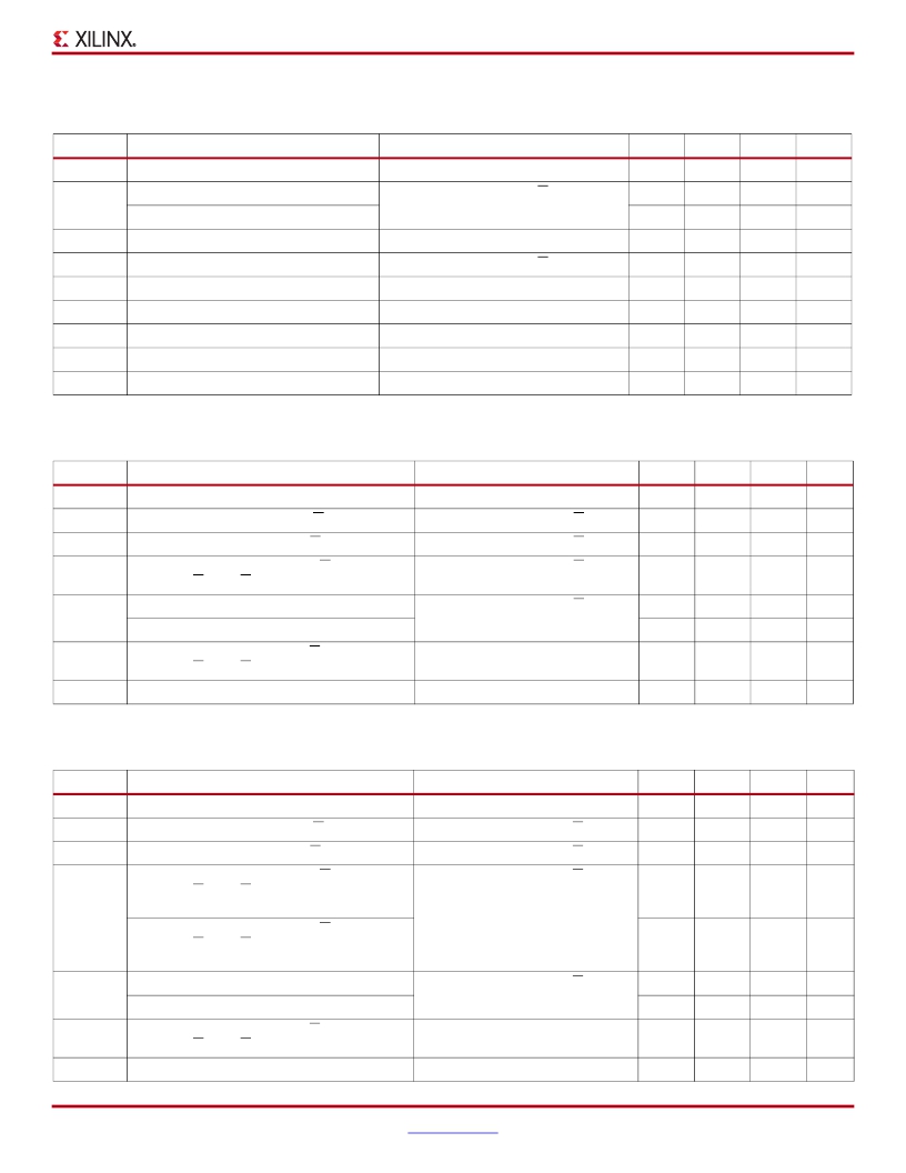
HT DC Specifications (HT_25)
Table 8: HT DC Specifications
Symbol
DC Parameter
Conditions
Min
Typ
Max
Units
V CCO
V OD
Δ V OD
Supply Voltage
Differential Output Voltage for XC devices R T = 100 Ω across Q and Q signals
Differential Output Voltage for XQ devices
Change in V OD Magnitude
2.38
480
480
–15
2.5
600
600
–
2.63
885
930
15
V
mV
mV
mV
V OCM
Δ V OCM
V ID
Δ V ID
V ICM
Δ V ICM
Output Common Mode Voltage
Change in V OCM Magnitude
Input Differential Voltage
Change in V ID Magnitude
Input Common Mode Voltage
Change in V ICM Magnitude
R T = 100 Ω across Q and Q signals
440
–15
200
–15
440
–15
600
–
600
–
600
–
760
15
1000
15
780
15
mV
mV
mV
mV
mV
mV
LVDS DC Specifications (LVDS_25)
Table 9: LVDS DC Specifications
Symbol
V CCO
V OH
V OL
V ODIFF
V OCM
V IDIFF
V ICM
DC Parameter
Supply Voltage
Output High Voltage for Q and Q
Output Low Voltage for Q and Q
Differential Output Voltage (Q – Q),
Q = High (Q – Q), Q = High
Output Common-Mode Voltage for XC devices
Output Common-Mode Voltage for XQ devices
Differential Input Voltage (Q – Q),
Q = High (Q – Q), Q = High
Input Common-Mode Voltage
Conditions
R T = 100 Ω across Q and Q signals
R T = 100 Ω across Q and Q signals
R T = 100 Ω across Q and Q signals
R T = 100 Ω across Q and Q signals
Min
2.38
–
0.825
247
1.075
1.000
100
0.3
Typ
2.5
–
–
350
1.250
1.250
350
1.2
Max
2.63
1.675
–
600
1.425
1.425
600
2.2
Units
V
V
V
mV
V
V
mV
V
Extended LVDS DC Specifications (LVDSEXT_25)
Table 10: Extended LVDS DC Specifications
Symbol
V CCO
V OH
V OL
V ODIFF
DC Parameter
Supply Voltage
Output High Voltage for Q and Q
Output Low Voltage for Q and Q
Differential Output Voltage (Q – Q),
Q = High (Q – Q), Q = High
Conditions
R T = 100 Ω across Q and Q signals
R T = 100 Ω across Q and Q signals
R T = 100 Ω across Q and Q signals
Min
2.38
–
0.715
350
Typ
2.5
–
–
–
Max
2.63
1.785
–
840
Units
V
V
V
mV
for XC devices
Differential Output Voltage (Q – Q),
350
–
850
mV
Q = High (Q – Q), Q = High
for XQ devices
V OCM
V IDIFF
V ICM
Output Common-Mode Voltage for XC devices
Output Common-Mode Voltage for XQ devices
Differential Input Voltage (Q – Q),
Q = High (Q – Q), Q = High
Input Common-Mode Voltage
R T = 100 Ω across Q and Q signals
Common-mode input
voltage = 1.25V
Differential input voltage = ±350 mV
1.075
1.000
100
0.3
1.250
1.250
–
1.2
1.425
1.425
1000
2.2
V
V
mV
V
DS152 (v3.6) March 18, 2014
Product Specification
9
发布紧急采购,3分钟左右您将得到回复。
相关PDF资料
EK-V7-VC707-CES-G
VIRTEX-7 VC707 EVAL KIT
EK-Z7-ZC702-CES-G
ZYNQ-7000 EPP ZC702 EVAL KIT
EL1848IYZ-T7
IC LED DRIVR WHITE BCKLGT 8-MSOP
EL7156CSZ
IC DRIVER PIN 40MHZ 3STATE 8SOIC
EL7158ISZ
IC DVR PIN 40MHZ 3STATE 8-SOIC
EL7222CSZ
IC DVR HS DUAL MOSFET 8-SOIC
EL7242CSZ
IC DVR HS DUAL MOSFET 8-SOIC
EL7243CMZ-T13
IC CCD DRIVER DUAL HS 20-SOIC
相关代理商/技术参数
EK-V7-VC707-CES-G
功能描述:VIRTEX-7 VC707 EVAL KIT RoHS:是 类别:编程器,开发系统 >> 通用嵌入式开发板和套件(MCU、DSP、FPGA、CPLD等) 系列:Virtex®-7 标准包装:1 系列:PICDEM™ 类型:MCU 适用于相关产品:PIC10F206,PIC16F690,PIC16F819 所含物品:板,线缆,元件,CD,PICkit 编程器 产品目录页面:659 (CN2011-ZH PDF)
EK-V7-VC707-CES-G-J
功能描述:VIRTEX-7 VC707 EVAL KIT JAPAN RoHS:是 类别:编程器,开发系统 >> 通用嵌入式开发板和套件(MCU、DSP、FPGA、CPLD等) 系列:Virtex®-7 标准包装:1 系列:PICDEM™ 类型:MCU 适用于相关产品:PIC10F206,PIC16F690,PIC16F819 所含物品:板,线缆,元件,CD,PICkit 编程器 产品目录页面:659 (CN2011-ZH PDF)
EK-V7-VC707-G
制造商:Xilinx 功能描述:VIRTEX-7 FPGA VC707 EVALUATION KIT - Boxed Product (Development Kits) 制造商:Xilinx 功能描述:KIT EVAL VIRTEX7 VC707 制造商:Xilinx 功能描述:VIRTEX-7 VC707 FPGA EVAL KIT
EK-V7-VC707-G-J
制造商:Xilinx 功能描述:KIT EVAL VIRTEX7 VC707 JAPAN
EKWF111
功能描述:WiFi/802.11开发工具 WF111 SDIO Eval kit
RoHS:否 制造商:Roving Networks 产品:Evaluation Boards 工具用于评估:RN-171 支持协议:802.11 b/g 频率:2.4 GHz 接口类型:UART 工作电源电压:2 V to 16 V
EKWT11-A
功能描述:蓝牙/802.15.1 开发工具 EKWT11-A
RoHS:否 制造商:Panasonic Electronic Components 产品:Bluetooth Evaluation Kit 工具用于评估:PAN1721 频率:2.4 GHz 接口类型:I2C 工作电源电压:2 V to 3.6 V
EKWT11-E
功能描述:蓝牙/802.15.1 开发工具 EKWT11-E
RoHS:否 制造商:Panasonic Electronic Components 产品:Bluetooth Evaluation Kit 工具用于评估:PAN1721 频率:2.4 GHz 接口类型:I2C 工作电源电压:2 V to 3.6 V
EKWT11i-A
功能描述:蓝牙/802.15.1 开发工具 WT11i A Eval Kit
RoHS:否 制造商:Panasonic Electronic Components 产品:Bluetooth Evaluation Kit 工具用于评估:PAN1721 频率:2.4 GHz 接口类型:I2C 工作电源电压:2 V to 3.6 V
